I love retro games and am fascinated by the clever tricks they use to overcome the extreme hardware limitations of early consoles. I therefore thought it would be a cool project to create an emulator for the NES, a classic 8-bit console with many great games. I had a lot of fun working on this project and learned a lot about the NES hardware. This post will discuss the different parts of the NES and how I went about implementing them.
By far the most essential resource for this project was the Nesdev Wiki, which contains all the information you could ever want about the NES hardware. I also found a great video series on NES emulation by javidx9 on YouTube which has some great visual explanations that were helpful for wrapping my head around some of the harder concepts, such as the PPU.
CPU
The CPU used by the NES is the 6502 microprocessor. This processor has an 8-bit data bus and a 16-bit address bus, meaning it has an addressable range of 0x0000 to 0xFFFF (hexadecimal), or 65536 bytes.
I started by defining a class for the CPU, encapsulating its internal registers and providing a public clock() function, for performing one clock cycle.
class Cpu
{
private:
    Bus *bus; // The bus. Used to route reads and writes to the correct components
    //                 NV-BDIZC
    uint8_t status = 0b00110100; // status register
    uint8_t a = 0;               // Accumulator register
    uint8_t x = 0;               // X register
    uint8_t y = 0;               // Y register
    uint8_t sp = 0xFD;           // Stack Pointer
    uint16_t pc = 0;             // Program Counter

    uint8_t cycles = 0; // Number of cycles until next instruction can be executed

    // Helper functions used by instructions to read/write memory
    uint8_t read(uint16_t addr);
    uint16_t read_u16(uint16_t addr);
    void write(uint16_t addr, uint8_t data);
    void write_to_next_address(uint8_t data, AddressingMode am);
    void stack_push(uint8_t data);
    uint8_t stack_pull();

public:
    Cpu();
    ~Cpu();

    // Signals that can be received by the CPU
    void clock(); // perform one clock cycle
    void reset(); // reset to a known state
    void irq();   // interrupt request
    void nmi();   // non-maskable interrupt

private:
    // Instruction functions (omitted)
}
The status register contains single-bit flags containing information about the processor's state, such as if an overflow occurred or an operation resulted in a negative number. The accumulator is used to store the results of arithmetic operations. The X and Y registers are general-purpose but have specific uses for some addressing modes. The stack pointer is a pointer to the top of the call stack in memory, and the program counter points to the memory location of the next instruction to be executed.
The clock function then looks something like this:
void Cpu::clock()
{
    if (cycles == 0)
    {
        uint8_t opcode = read(pc); // get the opcode at the address specified by the program counter
        pc++; // increment program counter

        // use lookup table which maps opcodes to instructions
        Instruction current_instruction = lookup[opcode];
        // set the number of cycles required by this instruction
        cycles = current_instruction.cycles;

        // perform the instruction
        bool extra_cycle = (this->*current_instruction.function)(current_instruction.addressing_mode);
        // some instructions require an extra cycle
        if (extra_cycle)
            cycles++;
    }
    cycles--;
}
I created a function for each instruction, each of which takes in an addressing mode and returns true if an extra cycle was required (this is often the case when a page boundary is crossed). The 6502 supports 11 different addressing modes, the simplest being immediate addressing in which the operand is the data to be operated on.
Bus
Earlier I mentioned that the CPU has an addressable range of 0x0000 to 0xFFFF, which implies that the NES has 64KiB of memory. In fact, the NES only has 2KiB of memory, accessed from 0x0000-0x1FFF. The rest of the addressable range is used to read and write data to the other components as shown in this diagram:

(side note: In this diagram I show the mapper as read-only, which is not the case for the more advanced mappers which have internal registers that can be written to. This is most commonly used to implement bank switching)
You may have noticed that the addressable range for memory is still too large. This is because the memory is mirrored four times. Mirroring is used all over the place by the NES and is basically when two or more memory addresses act on the same data.
I created a class that represents the bus, facilitating communication between components. For example, here is the read function for the bus, which you can see follows the above diagram:
uint8_t Bus::read(uint16_t addr)
{
    if (addr >= 0 && addr <= 0x1FFF)
    {
        // logical AND implements mirroring as it zeros left most bits
        return mem[addr & 0x07FF];
    }
    else if (addr <= 0x3FFF)
    {
        return ppu.read(addr & 0x0007);
    }
    else if (addr >= 0x8000 && addr <= 0xFFFF)
    {
        return cartridge.read(addr);
    }
    else if (addr == 0x4016)
    {
        // special address used to read controller state
        auto data = (controller_state[0] & 0x80) > 0;
        controller_state[0] <<= 1;
        return data;
    }
    return 0;
}
PPU
The Picture Processing Unit (PPU) is easily the most complicated part of the NES. It is a separate chip used to draw the graphics to the screen, having its own dedicated bus and memory. The PPU runs 3 times faster than the CPU, and each PPU clock cycle draws one pixel and moves the scanline to the right. Once it reaches the end of a scanline, it moves down to the next scanline.
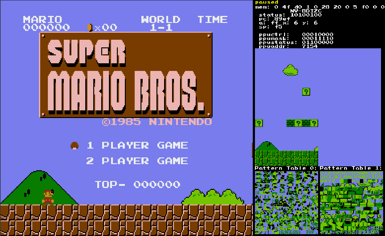
Along with the main graphics output, my emulator also shows some useful debugging information to the right, such as the contents of certain registers, a nametable, and the pattern tables. The pattern tables (shown in the bottom right) contain the tile and sprite graphics, where each is a 16x16 grid of 8x8 tiles. They allocate only 2 bits per pixel, meaning each tile can only display up to 4 colours (actually 3 + transparent). To get around this, each tile has a colour palette associated with it, mapping the 2-bit number to the specified colours.
The NES also has two nametables (logically it can address four nametables, but two of these are mirrors). These tell the PPU what tiles to draw where. The PPU can then smoothly scroll between these nametables to allow for levels that span multiple screens.
One surprising thing about the PPU is that it only has 9 registers that are accessible to the CPU. This means if the CPU wants to update an entry in the nametable it must write twice to the PPU's address register, which sets the 16-bit address to access, and then write to the PPU's data register to actually write the data. To speed up sequential reads or writes the address is auto-incremented whenever a read or write occurs.
This is just a high-level overview of the PPU, as there are many intricacies that I won't go into here.
Cartridges and Mappers
The CPU bus can read program ROM from the cartridge between addresses 0x8000 and 0xFFFF, and the PPU bus can read character ROM (pattern tables) from the cartridge between addresses 0x0000 and 0x1FFF. But what if a game needs more than 32KiB of program ROM or more than 8KiB of character ROM? The solution was to have a circuit within the cartridge that maps incoming addresses to different memory banks. This circuitry is called a mapper, and there are hundreds of different standards. Luckily most well-known games use the same 5-6 mappers.
To make it easy to add support for many different mappers I created an abstract Mapper class that can be inherited by any new mappers I decide to add:
class Mapper
{
public:
    Mapper(uint8_t prg_banks, uint8_t chr_banks);
    ~Mapper();

    /// Map the CPU address to the PGR ROM address
    virtual uint32_t map(uint16_t addr);

    /// Write to the mapper. Allows the mapper state to be changed
    virtual void write(uint16_t addr, uint8_t data);

    /// Map the PPU address to the CHR ROM address
    virtual uint32_t ppu_map(uint16_t addr);

protected:
    uint8_t num_prg_banks;
    uint8_t num_chr_banks;
};
NES cartridges use a standardized file format called iNES, which has a 16-byte header containing information such as the ID of the mapper used and the orientation the nametables should be mirrored.
This information is loaded into a Cartridge class. Reads and writes to the cartridge can then be implemented using the mapper like so:
uint8_t Cartridge::read(uint16_t addr)
{
    uint32_t mapped_addr = mapper->map(addr);
    return prg_rom[mapped_addr];
}

void Cartridge::write(uint16_t addr, uint8_t data)
{
    mapper->write(addr, data);
}

uint8_t Cartridge::ppu_read(u_int16_t addr)
{
    uint32_t mapped_addr = mapper->ppu_map(addr);
    return chr_rom[mapped_addr];
}
The last major part of the NES is audio synthesis, handled by a separate chip called the APU (Audio Processing Unit). At time of writing, audio is still work-in-progress, so I won't go into it for now.
The source code for this project available here